th Output of FF-3 i.e. This is why it is also known as a transparent latch - when Enable is asserted, the latch is said to be "transparent" - its signals propagate directly through it as if it isn't there. ti
When the flip-flops in a register are connected in such a way that the output of one flip flop, becomes the input of the other, a shift register is created.
The stored word is changed to 1100. Description of digital circuits in terms of flow of information between registers, Advantages of doing power estimation at RTL or architectural level, Learn how and when to remove this template message, "Power Estimation Techniques for Integrated Circuits ", "Low-Power Architectural Design Methodologies ", "Register-Transfer Level Estimation Techniques for Switching Activity and Power Consumption", "Power Macromodeling for High Level Power Estimationy", https://en.wikipedia.org/w/index.php?title=Register-transfer_level&oldid=1088743222, All Wikipedia articles written in American English, Short description is different from Wikidata, Articles needing additional references from December 2009, All articles needing additional references, Creative Commons Attribution-ShareAlike License 3.0.
It means that, the universal shift register can store the data in parallel and can transmit the data in parallel.
It is well known that more significant power reductions are possible if optimizations are made on levels of abstraction, like the architectural and algorithmic level, which are higher than the circuit or gate level [3] This provides the required motivation for the developers to focus on the development of new architectural level power analysis tools. But there is still a problem i.e. data is given separately to each flip flop and the output is collected in serial at the output of the end flip flop. Language links are at the top of the page across from the title. f When a number of flip flops are connected in series, this arrangement is called a Register.
We make use of First and third party cookies to improve our user experience.
lun t ho l mt thng hiu Vit Nam, Chng ti tin tng la chn tn min ".vn" bi ".vn" l
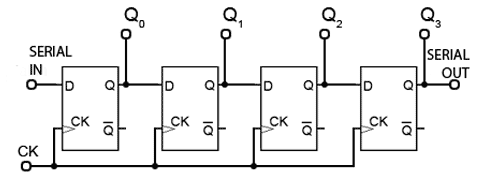
internal toggling on every propagation elapse completion. The clear (CLR) signal and clock signals are connected to all the 4 flip flops. Many of the digital system operations like division, multiplication are performed by using registers. i vi cc doanh nghip, t chc hay c nhn, website It is called Universal Shift Register as it can be used for left shift, right shift, serial to serial, serial to parallel, parallel to serial and parallel to parallel operations. This is because of the This enables the use of current limiting resistors to interface inputs to voltages in excess of VCC. Inputs include clamp diodes. The circuit diagram of a 4 bit bidirectional universal shift register is shown below. The output of the first flip flop is connected to the input of the next flip flop and so on. tr thnh mt cng c quan trng trong vic to dng s hin din v hot ng qung As the behavior of the JK flip-flop is completely predictable under all conditions, a form of memory that uses a series of flip-flops to store the individual bits of a binary word, such as a byte (8 bits) of data. denotes the activation frequency. So, the number of bits of the binary number is directly proportional to the number of flip flops.
Khi cha c website, tn min c th c s dng chuyn
Where N represents number of stages / flip flops and fC represents clock frequency. chn It is built using circuits called logic gates, each of which performs a different function. A register is basically a storage space for units of memory that are used to transfer data for immediate use by the CPU (Central Processing Unit) for data m
chn lm trang bn hng online vi tn min ".vn" m khng phi l cc ui WebThe General purpose registers are mainly stored data. Shift registers are basically a type of register which have the ability to transfer (shift) data. Registers are groups of flip-flops , where each flip-flop is capable of storing one bit of information. They may be the only option in designs that cannot afford gates for the relatively large logic circuit and signal routing needed for register data readback, such as the Atari 2600 games console's TIA chip. This leads to the problem that even if the model gives a correct estimate for the total power consumption by the chip, the module wise power distribution is fairly inaccurate. In the "Serial IN Parallel OUT" shift register, the data is passed serially to the flip flop, and outputs are fetched in a parallel way. The abstractions of the estimation techniques at a lower level can be used on a higher level with slight modifications. For example, if you use eight flip-flops at once, then you are A synchronous circuit consists of two kinds of elements: registers (Sequential logic) and combinational logic.
An n-bit register has a group of n flip-flops and is capable of storing binary information of n As soon as the next negative edge of the clock hits, FF-2 will set and the stored word change to Q3 Q2 Q1 Q0 = 1100.
For serial left operation, the input is applied to the serial input which goes to AND gate-1 shown in figure.
Registers are normally measured by the number of bits they can hold, for example, an "8-bit register" or a "32-bit register". hiu, v
Registers are generically storage devices which are created by connecting a specific number of flip flops together in series and the amount of data (number of bits) which can be stored by the register is always directly proportional to the number of flip flops, as each flip flop is capable of storing only one bit at a time.
The synthesis results are then used by placement and routing tools to create a physical layout. The input and outputs are connected through the combinational circuit.
The system can be kept bug free by updating the software. The Parallel in Serial our Shift Register is also called PISO Shift register. When we apply the first clock pulse to the arrangement; the second stage input changes to 1 and rest inputs are 0.
Your email is safe with us, we dont spam. In this register, the input is given in parallel and the output also collected in parallel.
IC 74498 8-bit bidirectional shift register with parallel inputs and three-state outputs. 1 to Din. A "Universal" shift register is a special type of register that can load the data in a parallel way and shift that data in both directions, i.e., right and left.
Unlike in netlist, constructs such as cells, functions, and multi-bit registers are available. f
They are.
To shift the data out serially, the WS control line is brought HIGH (Shift mode), the register then shifts the data out on clock input. Serial in Serial out Shift Register (SISO), 2.
But it also has its trade off as speedup is achieved on the cost of accuracy, especially in the presence of correlated signals.
Serial in parallel out registers are used for converting the data from serial form to parallel form.
In some situations it may be desirable to dictate when the latch can and cannot latch. Digital signals are discretization of analog signals. In digital electronics, a Register is a device which is used to store the information. The registers which will shift the bits to left are called Shift left registers. u {\displaystyle \displaystyle P_{\text{mult}}=K_{\text{mult}}N^{2}f_{\text{mult}}}.
The bidirectional shift register can be defined as The register in which the data can be shifted either left of right.
The time delay is usually calculated using the formula; N is the number of flip flop stage at which the output is taken, Fc is the frequency of the clock signal and t which is the value being determined is the amount of time for which the output will be delayed. The inputs D1, D2, D3 and D4 are connected in parallel and the outputs Q1, Q2, Q3 and Q4 are collected in parallel. What Are The Types Of Register In Electronics? serial in-scoping out (SISO) shift registers, storing data serially up to a certain point, while serial in-parallel out (SIPO) have data input serially, at a certain point, and at another specific point at the same time to reach their desired . Initially, all the flip-flops are set in "reset" condition i.e. To shift the data to right, the input is connected to the AND gate 1 of the first flip flop; through serial input pin.
The logic diagram of a 4 bit universal shift register is shown below.
This means when the data is read in, each read in bit becomes available simultaneously on their respective output line (Q0 Q3 for the 4-bit shift register shown below). A LOW on the master reset input (MR) clears the register and forces all outputs LOW, independently of other inputs. IC 7496 5-bit parallel-In/parallel-out shift register, asynchronous preset.
Privacy Policy. that for the formerly forbidden combination J=K=1 this flip-flop now performs
min khc.. As soon as a negative clock edge is applied, the input binary bits will be loaded into the flip-flops simultaneously.
The next bit of the binary number, i.e., 1, is passed to the data input D2. These are the applications of flip-flops. Even though a control line is now required, the SR latch is not synchronous, because the inputs can change the output even in the middle of an enable pulse. The next bit of the binary number, i.e., 1, is passed to the data input D1, and the clock is applied. When the Enable input is low, then the outputs from the AND gates must also be low, thus the Q and Q outputs remain latched to the previous data.
The data is shifted or transferred one bit at a time, when a clock pulse is applied. At this time, the first, third, and fifth gates will be activated, and the shifting of the data will be left to the right bit.
It is a technique based on the concept of gate equivalents. Frequently the two states can also be defined using Boolean logic functions, such as true or false states, or utilizing an on or off state.
K NCERT Solutions Class 12 Business Studies, NCERT Solutions Class 12 Accountancy Part 1, NCERT Solutions Class 12 Accountancy Part 2, NCERT Solutions Class 11 Business Studies, NCERT Solutions for Class 10 Social Science, NCERT Solutions for Class 10 Maths Chapter 1, NCERT Solutions for Class 10 Maths Chapter 2, NCERT Solutions for Class 10 Maths Chapter 3, NCERT Solutions for Class 10 Maths Chapter 4, NCERT Solutions for Class 10 Maths Chapter 5, NCERT Solutions for Class 10 Maths Chapter 6, NCERT Solutions for Class 10 Maths Chapter 7, NCERT Solutions for Class 10 Maths Chapter 8, NCERT Solutions for Class 10 Maths Chapter 9, NCERT Solutions for Class 10 Maths Chapter 10, NCERT Solutions for Class 10 Maths Chapter 11, NCERT Solutions for Class 10 Maths Chapter 12, NCERT Solutions for Class 10 Maths Chapter 13, NCERT Solutions for Class 10 Maths Chapter 14, NCERT Solutions for Class 10 Maths Chapter 15, NCERT Solutions for Class 10 Science Chapter 1, NCERT Solutions for Class 10 Science Chapter 2, NCERT Solutions for Class 10 Science Chapter 3, NCERT Solutions for Class 10 Science Chapter 4, NCERT Solutions for Class 10 Science Chapter 5, NCERT Solutions for Class 10 Science Chapter 6, NCERT Solutions for Class 10 Science Chapter 7, NCERT Solutions for Class 10 Science Chapter 8, NCERT Solutions for Class 10 Science Chapter 9, NCERT Solutions for Class 10 Science Chapter 10, NCERT Solutions for Class 10 Science Chapter 11, NCERT Solutions for Class 10 Science Chapter 12, NCERT Solutions for Class 10 Science Chapter 13, NCERT Solutions for Class 10 Science Chapter 14, NCERT Solutions for Class 10 Science Chapter 15, NCERT Solutions for Class 10 Science Chapter 16, NCERT Solutions For Class 9 Social Science, NCERT Solutions For Class 9 Maths Chapter 1, NCERT Solutions For Class 9 Maths Chapter 2, NCERT Solutions For Class 9 Maths Chapter 3, NCERT Solutions For Class 9 Maths Chapter 4, NCERT Solutions For Class 9 Maths Chapter 5, NCERT Solutions For Class 9 Maths Chapter 6, NCERT Solutions For Class 9 Maths Chapter 7, NCERT Solutions For Class 9 Maths Chapter 8, NCERT Solutions For Class 9 Maths Chapter 9, NCERT Solutions For Class 9 Maths Chapter 10, NCERT Solutions For Class 9 Maths Chapter 11, NCERT Solutions For Class 9 Maths Chapter 12, NCERT Solutions For Class 9 Maths Chapter 13, NCERT Solutions For Class 9 Maths Chapter 14, NCERT Solutions For Class 9 Maths Chapter 15, NCERT Solutions for Class 9 Science Chapter 1, NCERT Solutions for Class 9 Science Chapter 2, NCERT Solutions for Class 9 Science Chapter 3, NCERT Solutions for Class 9 Science Chapter 4, NCERT Solutions for Class 9 Science Chapter 5, NCERT Solutions for Class 9 Science Chapter 6, NCERT Solutions for Class 9 Science Chapter 7, NCERT Solutions for Class 9 Science Chapter 8, NCERT Solutions for Class 9 Science Chapter 9, NCERT Solutions for Class 9 Science Chapter 10, NCERT Solutions for Class 9 Science Chapter 11, NCERT Solutions for Class 9 Science Chapter 12, NCERT Solutions for Class 9 Science Chapter 13, NCERT Solutions for Class 9 Science Chapter 14, NCERT Solutions for Class 9 Science Chapter 15, NCERT Solutions for Class 8 Social Science, NCERT Solutions for Class 7 Social Science, NCERT Solutions For Class 6 Social Science, CBSE Previous Year Question Papers Class 10, CBSE Previous Year Question Papers Class 12, Classwise Physics Experiments Viva Questions, Advantages of Digital System over Analog System, CBSE Previous Year Question Papers Class 10 Science, CBSE Previous Year Question Papers Class 12 Physics, CBSE Previous Year Question Papers Class 12 Chemistry, CBSE Previous Year Question Papers Class 12 Biology, ICSE Previous Year Question Papers Class 10 Physics, ICSE Previous Year Question Papers Class 10 Chemistry, ICSE Previous Year Question Papers Class 10 Maths, ISC Previous Year Question Papers Class 12 Physics, ISC Previous Year Question Papers Class 12 Chemistry, ISC Previous Year Question Papers Class 12 Biology, JEE Main 2023 Question Papers with Answers, JEE Main 2022 Question Papers with Answers, JEE Advanced 2022 Question Paper with Answers.
Below is the diagram of 4-bit "bidirectional" shift register where DR is the "serial right shift data input", DL is the "left shift data input", and M is the "mode select input".
The diagram of the universal shift register is given below.
IC 74166 parallel-Load 8-bit shift register.
AND1 OR 1 FF 1 Q1 AND 2 OR 2 FF 2 Q2 AND 3 OR 3 FF 3 Q3 AND 4 OR 4 FF 4 Q4 (Serial Data OUT).
When the shift/load bar line is low (0), the AND gate 2, 4 and 6 become active they will pass B1, B2, B3 bits to the corresponding flip-flops. Circuit components acting like computer memory, Advanced Configuration and Power Interface, Learn how and when to remove this template message, http://www.microsoft.com/whdc/resources/MVP/xtremeMVP_hw.mspx#ETB, Microsoft "Guidelines for Bus and Device Specifications", https://en.wikipedia.org/w/index.php?title=Hardware_register&oldid=1144699159, All Wikipedia articles written in American English, Wikipedia introduction cleanup from June 2015, Articles covered by WikiProject Wikify from June 2015, All articles covered by WikiProject Wikify, Articles with unsourced statements from March 2023, Articles needing additional references from August 2016, All articles needing additional references, Creative Commons Attribution-ShareAlike License 3.0, This page was last edited on 15 March 2023, at 03:01.
gii, ti s dng tn min .vn nh mt li khng nh v xut x thng Gi denoting the hardware complexity of the multiplier is related to the square of the input word length i.e. In such types of operations, the data is entered serially and taken out in parallel fashion.
There are two common types of registers: Parallel load Register. As in analog thermometers, the thermistor in the probe is isolated from the patient by a probe cover.
The input to this register is given in serial and the output is collected in parallel. Taking care of analog issues in digital systems could be demanding as analog components are used in designing the digital system.
The clock input is directly connected to all the flip flops but the input data is connected individually to each flip flop through a mux (multiplexer) at input of every flip flop.
Apart from the above register types we have the other type of registers also. The shift register can be used for temporary storage of data. IC 74164 8-bit parallel-out serial shift register with asynchronous.
The D latch outputs the 'D' input whenever the Enable line is high, otherwise the output is whatever the D input was when the Enable input was last high.
Generally shift registers are available in 4000 series and 7000 series ICs. These components are divided into two categories: The active components are the transistors and diodes, while passive components are the capacitors, resistors, inductors, etc.
A register, in its widest sense, is a collection of flip flops connected by gates that control their functioning.
Inputs are overvoltage tolerant to 15 V. This enables the device to be used in HIGH-to-LOW level shifting applications.
The binary is a radix-2 number system having 2 different digits: 0 and 1. IC 74671 4-bit bidirectional shift register. Q1, Q2, Q3 and Q4 are the outputs of first, second, third and fourth flip flops, respectively. The decimal number system is radix-10, having 10 different digits or symbols.
A semiconductor device with three terminals is known as a transistor. Learn more. The data is transferred through serial shift registers and other type.
K
u tin ca ti l tn min highteastory.vn cho thng hiu ca mnh.
Your email address will not be published. SPIRIT IP-XACT and DITA SIDSC XML define standard XML formats for memory-mapped registers.[4][5][6].
As a matter of fact activity factors will vary throughout the chip hence this is not very accurate and prone to error.
This register has mode input for right shift or left shift, a clock signal and two serial Data lines one each for input and output.
Shift Registers are sequential logic circuits, capable of storage and transfer of data.
Trenton Bureau.
WebMDR is the register of a computer s control unit that contains the data to be stored in the computer storage (e.g. So this is called Ring Counter.
This page was last edited on 10 January 2023, at 07:50. Register in Sequential Circuits So, we have discussed the operation of how a sequential circuit works.
The flip flops are connected in such a way that the first flip flop's output becomes the input of the other flip flop.
The series of data bits are stored by registers is called Byte or Word where a Byte is collection of 8 bits and a Word is collection of 16 bits (or 2 Bytes). WebA shift register is a register which is able to shift or transfer it content within itself without changing the order of the bits. This register can perform three types of operations, stated below. But the main use of a SISO is to act as a delay element. EX-OR and EX-NOR are the special gates. The outputs are disabled as long as the data is loading. Depending on their complexity, modern hardware devices can have many registers.
This helps ensure that the data stays longer (as long as it stays in read mode).
Advanced Navigation, a developer of artificially intelligent (AI) robotics and navigation technology, and KKR, a global investment firm, have signed a definitive agreement under which KKR will lead a AUD 108 million (USD 68 million) Series B funding round in Advanced Navigation.
Like a finite memory machine, the next state of the device is always determined by shifting and inserting a new data into the previous position.
In addition, the course will use other components that are all standard but put together in various combinations to achieve the desired result. A group of flip flops which is used to store multiple bits of data and the data is moved from one flip flop to another is known as Shift Register.
Thus the parallel in serial out operation takes place.
The binary data in a register can be moved within the register from one flip-flop to another. = Your Mobile number and Email id will not be published. A register is a group of binary cells suitable for holding binary information.
This register can be used to store and shift a 4-bit word, with the write/shift (WS) control input controlling the mode of operation of the shift register.
With mode control pin connected to ground, the universal shift register acts as a bi-directional register.
trng.
Other than counting, these are used for measuring the frequency as well as time. IC 74291 4-bit universal shift register, binary up/down counter, synchronous. The states Motor Vehicle Commission said Monday it will allow drivers to begin registering vehicles on digital platforms.
The loaded bits will appear simultaneously to the output side. doanh nghip nhp khu v phn phi hng quc t, vic ng k tn min cng gip The input to this register is given in serial fashion i.e.
The inverter is connected from the output, Q, of a register to the register's input, D, to create a circuit that changes its state on each rising edge of the clock, clk. Parallel in Parallel out Shift Register (PIPO), 4.
Designers can implement registers in a wide variety of ways, including: In addition to the "programmer-visible" registers that can be read and written with software, many chips have internal microarchitectural registers that are used for state machines and pipelining; for example, registered memory. t The set of Flip-flops is nothing but a register, used to store numerous data bits. If this input set to 0, then the serial shifting operation is performed. A 4-bit SISO shift register consists of 4 flip flops and only three connections. Logic simulation tools may use a design's RTL description to verify its correctness.
Zoo Miami Summer Camp 2022, Jeanine Mason And Camila Cabello, Articles W